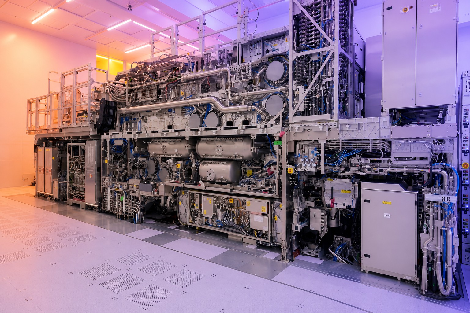
ASML has secured commitments from the largest chipmakers to adopt its newest production technology, Bloomberg reports. Samsung will use High-NA EUV lithography for mass production from 2028 and TSMC from 2030, joining Intel, which already runs the machines at roughly $400 million each. The substantive part of the agreement is smaller and stranger than the machine purchases: all four companies plan to move from today's six-inch photomasks to 12-inch ones, a change ASML says can raise High-NA throughput by 40%.
ASML is still the only company in the world that builds EUV lithography equipment, the machines required to make the most powerful AI accelerators. It brought the simpler Low-NA generation to market in 2019 and has since been working with customers to bring the harder High-NA systems into production.
A photomask is the stencil that carries the chip's circuit pattern. During lithography, light passes through it onto a silicon wafer coated with photosensitive material and transfers the pattern that becomes the transistors and wiring. A bigger mask means more area printed per exposure. The six-inch ceiling has capped how large a single chip can be, which is why manufacturers have had to stack several dies vertically and build complicated schemes for getting them to talk to each other — more cost, more design complexity, for a constraint that comes from the size of a piece of glass.
Moving to 12-inch masks has long been treated as difficult and expensive. Marco Pieters, ASML's chief technology officer, says coordinated action across the four companies can lift High-NA productivity by 40% and simplify chip design, and he called the transition a major opportunity. TSMC and ASML plan to build a test line for 12-inch masks by 2031, with production use on High-NA machines from 2033.
TSMC's position here has reversed. Until now it held that the productivity gain did not justify the extra spending. It has changed its mind, which matters more to ASML than the others: TSMC accounts for about 16% of the company's revenue. Samsung, one of the largest memory makers, intends to start using High-NA for memory chips in 2028, at a moment when memory prices are climbing sharply on demand from AI data centres.
While ASML consolidates its customers, Huawei is working to get them out of the chain entirely. The Financial Times reports that the company is trying to strip foreign technology out of China's semiconductor supply chain and route around Western export controls on ASML equipment, investing across every link of the lithography chain and helping broker agreements with leading manufacturers, SMIC among them.
China's effort is not aimed at EUV. It is aimed at DUV — deep ultraviolet, at a wavelength of 193 nanometres, against EUV's 13.5. The shorter wavelength is what makes the finest structures and the most advanced chips possible. DUV is the older, mature technology on which most of the world's chips are made, and with multipatterning, where a pattern is built up over several successive exposures, it can produce more complex semiconductors too. It just takes more time, more effort and more money than doing it with EUV.
At the centre of Huawei's push is Yuliangsheng, a Shanghai equipment maker that the FT reports helped develop China's first modern DUV machine. Yuliangsheng was spun out of SiCarrier, which the paper links to Huawei; Huawei denies the connection. SMIC is testing the machine and Huawei uses it on its own lines, so far for less advanced semiconductors. Yuliangsheng expects to produce 12 DUV machines by the end of the year and remains far behind ASML.
Lin Qingyuan, an analyst at Bernstein, describes Huawei's role in the Chinese DUV programme as that of project manager. One prototype is not an industry: that takes thousands of suppliers and customers, and a central force to coordinate them.
What ASML actually announced, read closely, is a calendar rather than an order book. Samsung in 2028, TSMC in 2030, a test line in 2031, masks in production in 2033. There are no machine counts, no volumes, no numbers a customer could be held to — and the furthest date sits seven years out, which in this industry is long enough for two more arguments about whether the economics work. But the calendar is the point. The reason six inches has held for so long is not that nobody could build a larger mask; it is that a mask transition only pays if everyone moves at once, and no single company can decide that alone. ASML has spent years unable to buy that agreement. It now has it from all three of its biggest customers.
The more interesting question is what changed at TSMC. The reporting gives the reversal and not the reason, and the physics of the 40% has not moved. My read is that the arithmetic moved instead: when a single accelerator die is worth what it is worth today, the cost of stitching dies together stops looking like an engineering nuisance and starts looking like margin. Nobody at ASML said that, and nobody at TSMC was asked.
There is a quieter sentence in the Huawei half of this story. Yuliangsheng uses Zeiss lenses, according to the FT. Zeiss says it sells optics only to ASML. The FT's sources point to the secondary market — which is to say that the single hardest component in the chain, the one export controls are built around, is reaching Shanghai anyway, through a channel nobody has to approve. Huawei's venture arm Habo is simultaneously funding a Zeiss competitor, Fujian Zhiqi Photonics, and the light source developer Beijing RSLaser, which is a reasonable inference about how long the secondary market can be relied on.
Both halves of this story rest on the same judgement: that the binding constraint in lithography is no longer any one machine but the number of companies that have to agree to change together. ASML just got three of them to say yes to a date in 2033. Huawei is trying to assemble thousands from scratch, one lens supplier at a time.