
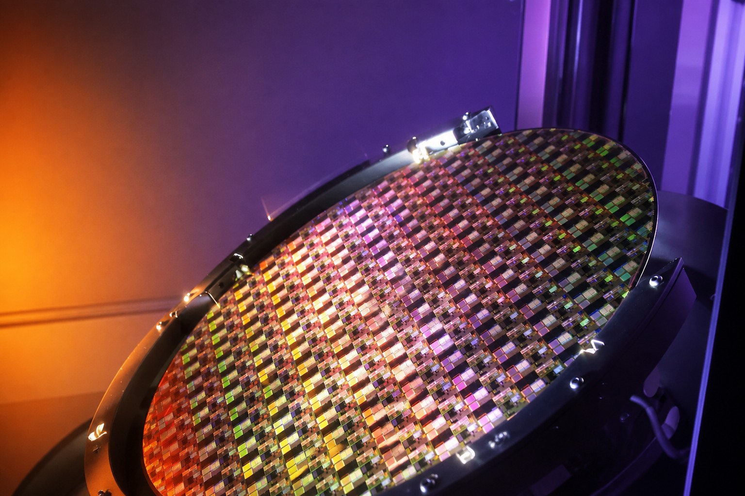
Kepler Computing, a San Jose company founded in 2018 by a team of physicists and computer scientists, has spent more than seven years in stealth rearranging the architecture of computer memory. It now says its approach can ease the global shortage of memory chips — if it can be manufactured in volume. The pitch is a supply argument rather than a performance one: Kepler claims a high-bandwidth memory design that raises density without extreme ultraviolet lithography, and that runs in semiconductor plants that already exist. The company has raised $468 million, and in July the US Commerce Department committed up to $245 million toward building the technology domestically.
EUV is the expensive part of modern chipmaking. It is how manufacturers shrink transistors and fit more onto the same area, and it is one of the reasons memory capacity cannot simply be conjured when demand spikes. Kepler says its 3D assembly and a patented material get the density gains without it.
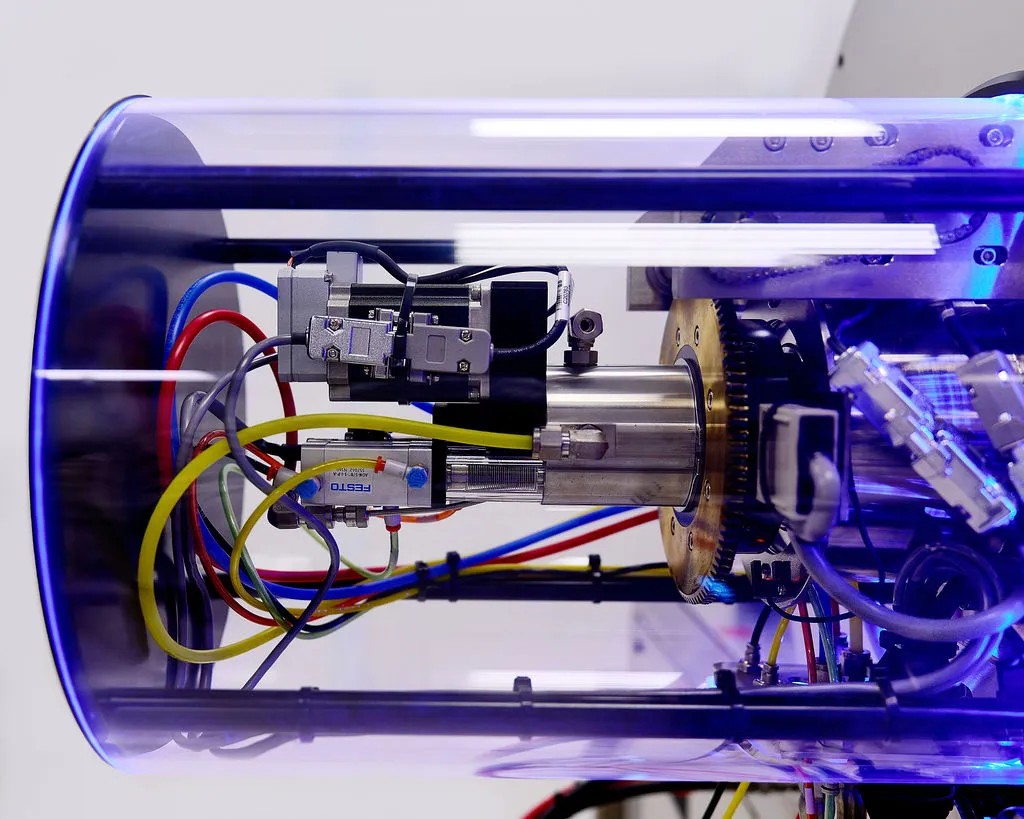
The work splits in two. For HBM, Kepler developed a 3D manufacturing technique that places more memory dies in a fixed area and lets the compute core sit closer to the memory, so moving data costs less energy. The stated goal is to bring HBM's data-movement energy toward SRAM levels while keeping HBM's much larger capacity. HBM is built from stacks of DRAM, a separate component; SRAM is the fast cache that sits inside the die of CPUs, GPUs and XPUs to shorten data transfer times. Kepler says it has made comparable progress on SRAM, raising its density using ferroelectrics, which read and write at lower voltage than the mechanisms semiconductors normally use to process and store data. To do that the startup built a new low-voltage composite material compatible with the ferroelectric approach.
Sasi Manipatruni, Kepler's cofounder and CTO, says the team tested 35 composite variants before settling on a class of materials it believes will make memory chips simpler and cheaper to produce. The sequence, as he describes it, was to solve the physical problem behind HBM's limits first, then develop the material that increases the amount of memory between chips.
Source: wired.com
The density claim is specific: Kepler says it can produce SRAM at densities comparable to chips built on 2nm and 3nm nodes, without ever buying an EUV scanner.
The economic argument is where the company is most pointed. A new memory fab, built and equipped, costs $20–40 billion, before equipment running into the hundreds of millions on top. In early work with GlobalFoundries, Kepler says it converted an existing fab into a next-generation facility in eight months; the usual timeline is 24. Debo Olaosebikan, cofounder and CEO, frames the strategy as using fabs and architectures that are already standing and pushing them to their physical limits.
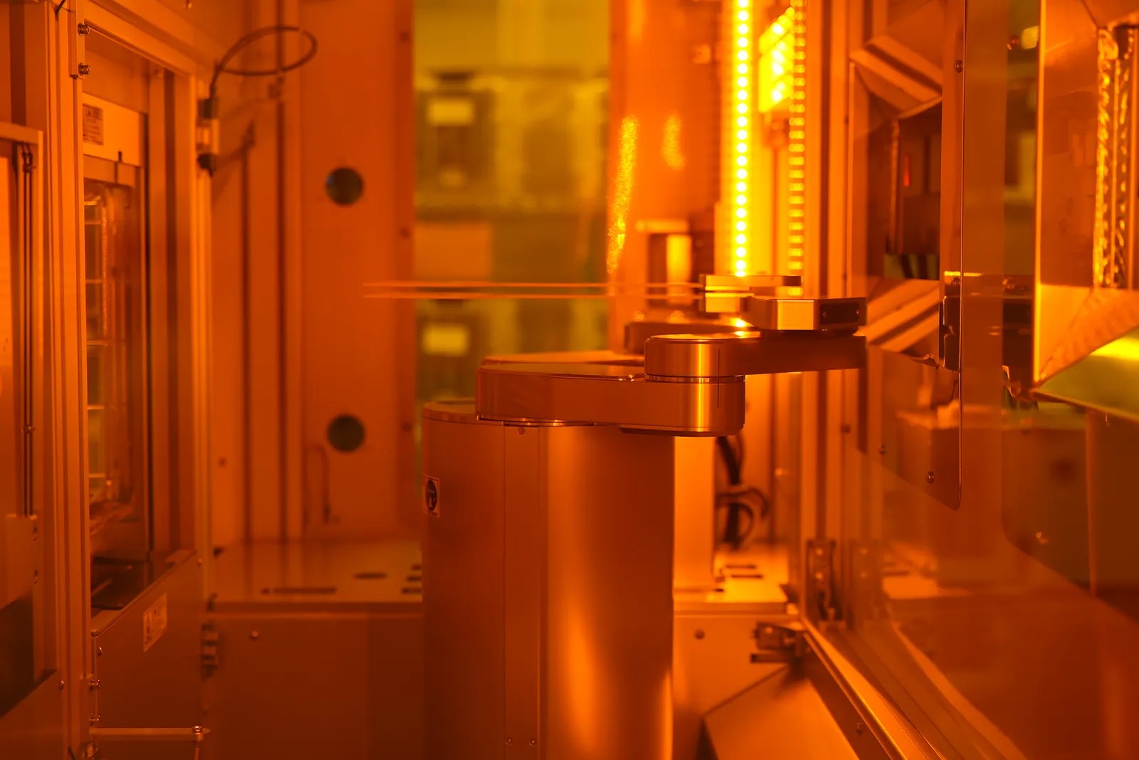
GlobalFoundries is both Kepler's manufacturing partner and a $50 million investor. Much of the testing runs at its plant in Singapore, where over the past two years Kepler has built what it calls mini-fabs and produced memory chips alongside GlobalFoundries' 28nm parts. More testing runs at the company's site in Burlington, Vermont. Ed Kaste, GlobalFoundries' senior vice president for CMOS, says the approach fits his company's strategy — a new materials system that can scale across several generations without rebuilding the fab or buying very expensive lithography equipment.
Source: wired.com
The rest of Kepler's money comes from Intel Capital, AMD Ventures, the British investment fund Baillie Gifford, and Bill Gates through his private Gates Frontier fund. Srini Anant, a managing director at Intel Capital, says the plan was never to replace DRAM or SRAM: the market was supposed to decide the direction, and demand has now appeared for both.
That is a tidier account than the actual history. Olaosebikan says Kepler originally intended to do SRAM first and move to DRAM and HBM later. ChatGPT launched in 2022, demand for an alternative to HBM jumped, and the roadmap was rewritten: SRAM and HBM are now developed in parallel. The shortage that Kepler presents as validation is also what reordered its product plan.
Meanwhile SK Hynix and Micron are rushing multi-billion-dollar fabs into existence, betting that even once those open, the market will still be short of high-bandwidth memory. Kepler's argument is that the accelerated-computing market should not have to wait for any of that — supply can grow through new ways of making memory inside plants that are already running.
Here is what I think the announcement actually shows. The technical endorsements in it come from GlobalFoundries, which manufactures the chips and holds equity, and from Intel Capital, which holds equity. That is not disqualifying, but it means the independent read on Kepler's claims is currently one analyst who says he does not know the details. And the timeline lands after the problem. Kepler has tested on roughly 2,000 silicon wafers. It plans to ship the first HBM sample chips later this year, ramp production in Singapore next year, and begin making chips in the US in 2028. A memory shortage that the industry is spending tens of billions to fix now will be resolved, one way or another, before Kepler's US line exists.
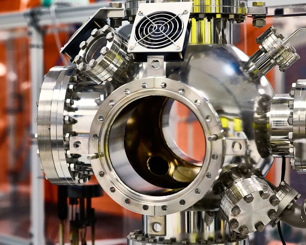
Kaste's own framing is the honest one: the major technological breakthroughs, he believes, are done, and what remains is getting stable results across thousands of wafers and millions of devices. That gap — 2,000 wafers to millions of devices — is where most novel materials die. Kepler's has a specific hazard in it: iron. Iron is difficult to bring into a fab because it can act as a contaminant, so the technology has to run on dedicated equipment or inside a fully sealed enclosure that keeps the material from escaping. Kaste says the key task is reliably isolating it at every stage of production. Olaosebikan declined to name the elements in the composite, saying only that the company uses a small number of materials, some of them not typically found in common ferroelectrics.
Source: wired.com
The more interesting question is the one the announcement leaves alone: cost per bit. Kepler's entire case is that retrofitting existing fabs is cheaper than building new ones, and the company expects the extra spending on new materials and retooling to come in far below the price of a greenfield plant. But no yield figure appears anywhere, no cost comparison against a DRAM stack from SK Hynix or Micron, and no customer is named for the samples shipping this year. Dedicated equipment and hermetic containment are not free, and a process that needs isolated tooling is structurally harder to make cheap than one that does not. A supply-side pitch without a price is a physics claim, not a business one.
Kepler is not the only startup trying to rearrange semiconductor manufacturing. Late last year the well-funded Substrate drew attention with a lithography approach using nanoparticles to deposit features on advanced chips; some industry analysts were skeptical, telling Bloomberg it would be extremely difficult for Substrate to produce large volumes of chips meeting very tight requirements, on schedule and on budget. Austin Lyons, a chip analyst at Creative Strategies who is not familiar with the details of Kepler's work, stated the general problem plainly: an innovation has to clear the constraints of contamination, mixed materials and mixed equipment before it can be applied at volume, and its cost has to justify the result.
Kepler has $468 million, a government commitment, a fab partner and a materials system nobody else is using. What it does not yet have is a single wafer lot at volume yield. Inventing a new way to make memory is one problem. Meeting historically high demand for it is a different one, and the second is the one that pays.